
Drying MEMS Wafers with Infrared
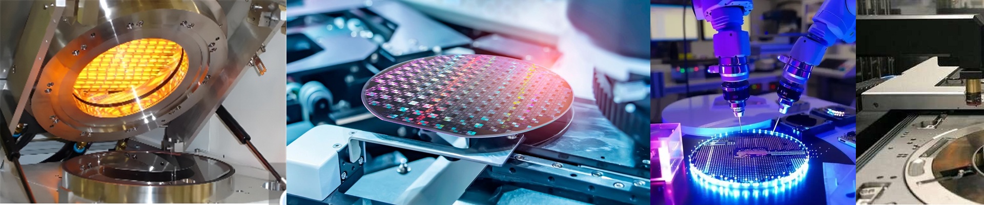
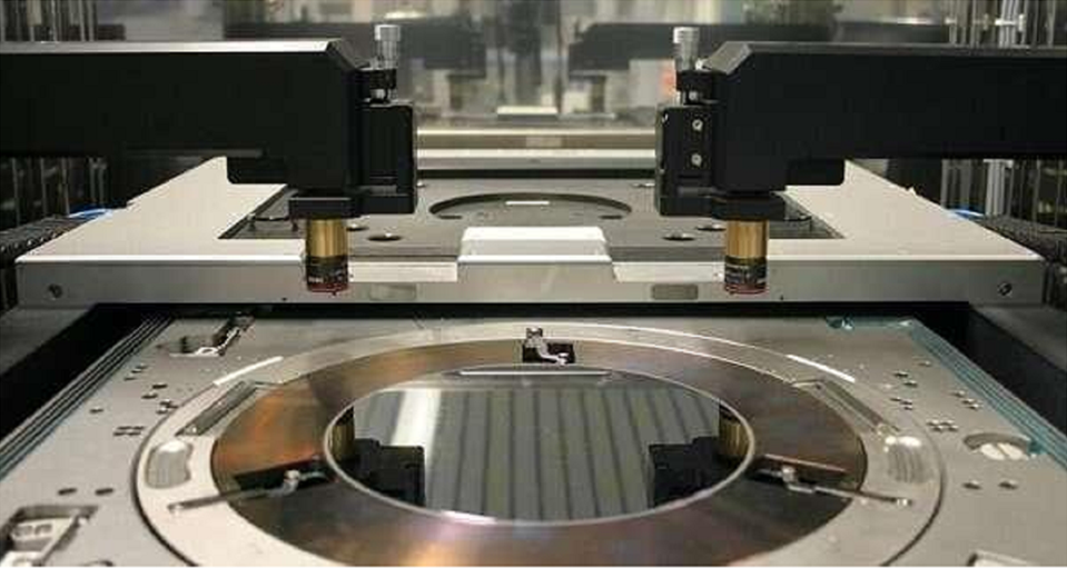
When you’re drying MEMS sensor wafers, you’ve got a tricky balance to strike. You need the moisture gone, but you can’t leave any residue behind, and you definitely can’t stress the hardware. That’s why we lean on infrared (IR) curing. Instead of messing around with chemicals or heating up the air, IR radiation hits the water molecules directly. It’s a cleaner way of doing things, and it fits right in with the move toward eco-friendly, lead-free standards in the fab. How it actually works Think about a standard convection oven. You have to heat the whole chamber, which takes forever. With IR, we target the wafer surface. We use short-wave or medium-wave spectrums so the energy can punch through those thin MEMS films and evaporate liquids almost instantly. The best part? There’s no waiting an hour for the oven to pre-heat. You just turn it on and go. The engineering side of things We usually go with quartz-halogen elements. Quartz is great because it doesn’t freak out under high thermal shock, and the halogen cycle keeps the lamps from burning out too quickly. But you have to be careful. If you dump too many watts into a tiny area, you’ll warp the wafer or fry the delicate sensor membranes. It’s a tightrope walk. That’s why we tune our PID controllers for millisecond response times. We need that surface temperature to stay exactly where it belongs. Why bother with IR? If you use hot air, you’re basically blowing contaminants right into the MEMS cavities. It’s a mess. IR is non-contact. No airflow, no drifting particles—just clean, dry heat. There is one catch, though: line-of-sight. IR only heats what it can “see.” If your wafer carrier has a weird shape, you’ll end up with cold spots. To fix that, we use arrays of lamps and reflective housings. It makes sure the heat hits every single millimeter of the wafer. It stops energy waste and shrinks the drying cycle down to a few seconds.