
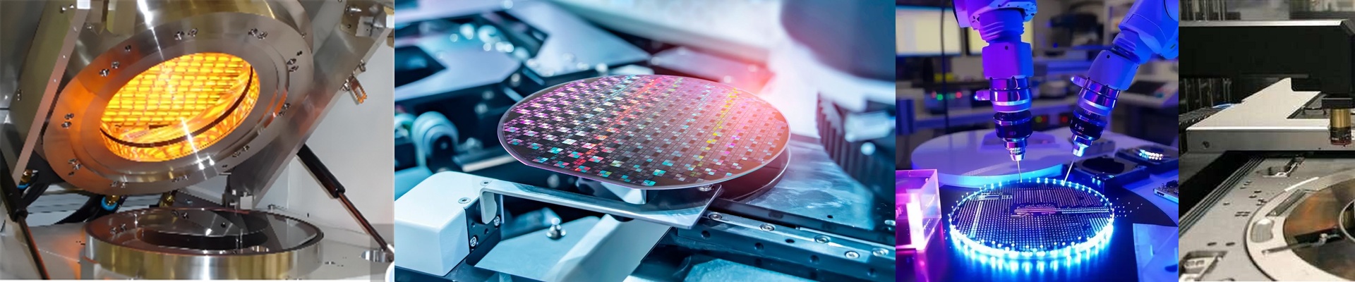
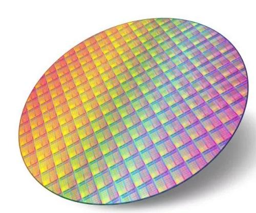
On the line, the clock doesn’t wait for thermal drift to settle. A wafer comes out of the clean rinse, beads still clinging to the edge. The photoresist is waiting for a soft bake that has to land within a degree—not a range. In the back end, encapsulants and underfills need a cure profile that holds shift after shift. Heat isn’t a background parameter here. It is the process. When the heat wavers, you see it fast: skin effect across the wafer, residual solvent trapped in the resist, weak bonds in the package. Scrap climbs. Rework climbs. Schedules slip. We built our advanced packaging infrared lamp system for that reality. It’s engineered around the four thermal moments that make or break yield in semiconductor manufacturing: wafer drying, photoresist baking (soft bake and hard bake), packaging curing, and post-clean drying.
What matters, technically
Infrared heating is fast, but speed means nothing without control. The system uses near-infrared (NIR) emitters tuned to match how silicon, photoresist, and common encapsulants absorb energy. You get direct transfer into the film or substrate, not wasted heat on fixtures and chamber walls. The specs were chosen to match semiconductor process windows, not lab ideals:
- Temperature uniformity: ±0.1°C across the active zone, verified by mapping under production airflow.
- Photoresist bake precision: setpoint stability of ±0.5°C through the full bake cycle, ramp and soak included.
- Cleanroom compatibility: rated for Class 1–100 environments, with sealed housing, low outgassing materials, and no exposed filaments.
- Particle performance: zero particle generation during operation, measured at the wafer surface with ISO-classified particle counters.
- Reliability: 24/7 continuous operation with zero unplanned downtime in documented deployments, backed by emitter life monitoring and predictive maintenance alerts.
- Repeatability: recipe-driven control with traceable setpoints, so the same thermal profile runs lot to lot, tool to tool. The lamp head pairs a short-wave infrared element with a reflector geometry that keeps the beam tight on the target, minimizing stray heat on nearby optics and sensors. Power delivery is sized to the substrate’s thermal mass—thin-film carriers to thick mold compounds—without overshoot. And control isn’t left to operator feel. Closed-loop temperature control runs off calibrated sensors positioned at the work plane, not in a remote housing. Recipes lock in ramp rates, soak times, and cooldown thresholds, so the process runs the same at 3 a.m. as it does at 3 p.m.
Why it works where it matters
Wafer drying
After wet cleaning, water marks show up when the film cools too slowly or unevenly. The infrared lamp dries wafers in seconds with uniform heat across the surface. The profile is aggressive enough to drive off moisture, yet controlled enough to protect delicate low-k films. You end up with a dry, spot-free wafer and consistent edge-to-center behavior, and cycle time improves because the bake step stops being a bottleneck.
Photoresist baking (soft bake and hard bake)
In lithography, the soft bake sets resist viscosity and removes solvent. The hard bake locks the image and preps the surface for etch or plating. Temperature accuracy and uniformity directly impact critical dimension control and sidewall profile. The lamp holds the bake within ±0.5°C of the recipe, with fast stabilization after door open/close events. The payoff is predictable critical dimension across the wafer and across the lot, and fewer reworks from footing or scum.
Packaging curing
Advanced packaging materials cure inside narrow thermal windows. Overheat and you get voids and delamination. Undercure and you get weak joints and reliability risk. The infrared system cures encapsulants, underfills, and adhesives with repeatable profiles that track the material’s exotherm behavior without hot spots. Heat goes where it’s needed—right on the joint—cutting total energy per unit while staying inside the required thermal budget.
Cleaning and drying
Post-clean drying has to strip rinse residues without adding contamination. The lamp delivers rapid, clean drying that doesn’t depend on compressed air or contact wiping. With zero particle generation and cleanroom-compatible construction, the process stays in spec, and maintenance stays lighter because there are no consumables to swap after every cycle. Across these steps, the gains are measurable:
- Yield protection: tight thermal control reduces variability in photoresist and cure, keeping the process inside design rules.
- Energy efficiency: direct IR heating cuts wasted energy on fixtures and chambers, lowering power draw per wafer.
- Throughput: faster ramp and soak times shorten cycle time without compromising profile integrity.
- Tool uptime: emitter life monitoring and modular design shrink maintenance windows, keeping the line moving.
The practical stuff you need to plan for
Infrared lamps are compact, but they aren’t plug-and-play.
- Integration footprint: Plan for airflow, clearance, and thermal isolation. The reflector needs line-of-sight to the target, and stray heat has to be managed so you don’t cook adjacent sensors or polymer components.
- Emitter replacement planning: Emitters have a finite life. Treat replacement as preventive maintenance, not emergency downtime. Our predictive alerts help, but you still need to schedule the work.
- Process matching: Every material set—resist, encapsulant, underfill—responds differently to IR wavelength and intensity. Qualification should start with a thermal profile review and a short design-of-experiments to lock the recipe.
- Cleanroom behavior: The system is built for low outgassing and zero particle generation, but it still radiates heat. Make sure nearby plastics, adhesives, and seals are rated for the local temperature environment. We design and qualify this lamp for semiconductor production. We run it in the same environments you do—Class 1–100 cleanrooms, high-mix lines, and 24/7 schedules. The numbers are specific because the process is specific. If thermal steps are driving scrap, variability, or schedule risk, specify the advanced packaging infrared lamp for wafer drying, photoresist baking, and curing. We’ll map performance, lock the recipe, and keep the line running without thermal excuses.